Unlike the software community, the hardware community tends to use extremely expensive, licensed toolchains such as Quartus, Vivado, and other EDAs from Synopsys and Mentor Graphics. Open source tools exist, but, meh… 🙂
Earlier this week I was using verilator to simulate a toy project, which uses an IP from Intel/Altera called altsyncram, a widely used block ram module for Intel/Altera FPGAs. This IP is provided in Quartus’s simlib as a huge verilog file (so other EDA tools like VCS and ModelSim can use it to simulate FPGA projects). After a bunch of hacking (i.e., turning off errors and warnings), I got it compiled. However, this module never gives a meaningful read response. The problematic code can be summarized as follow:
module testram(
    input logic clk,
    input logic wen,
    input logic [3:0] waddr,
    input logic [15:0] wdata,
    input logic [3:0] raddr,
    output logic [15:0] rdata
);

    altsyncram #(
        .intended_device_family("Stratix"),
        .operation_mode("DUAL_PORT"),
        .width_a(16),
        .widthad_a(4),
        .numwords_a(16),
        .width_b(16),
        .widthad_b(4),
        .numwords_b(16),
        .rdcontrol_reg_b("CLOCK0"),
        .address_reg_b("CLOCK0"),
        .outdata_reg_b("UNREGISTERED"),
        .read_during_write_mode_mixed_ports("OLD_DATA")
    ) bram (
        .clock0(clk),

        .wren_a(wen),
        .address_a(waddr),
        .data_a(wdata),
        .rden_a(0),

        .address_b(raddr),
        .q_b(rdata),
        .wren_b(0),
        .rden_b(1),

        .data_b(),
        .clock1(),
        .clocken0(),
        .clocken1(),
        .clocken2(),
        .clocken3(),
        .aclr0(),
        .aclr1(),
        .byteena_a(),
        .byteena_b(),
        .addressstall_a(),
        .addressstall_b(),
        .q_a(),
        .eccstatus()
    );
endmodule
In this module, I configured altsyncram as duo-port BRAM, where the first port only serves write and the second port only serves read.
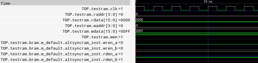
Then, I got the following waveform:
In the testbench, I set raddr to 0, waddr to 0, and wdata to 0xff, so hopefully 0xff will be written to the BRAM, and the value can be read out through rdata. From the code, we can see that testram.wen is obviously connected to testram.bram.m_default.altsyncram_inst.wren_a (because we use this port to write). However, verilator does not propagate the signal to it. Also, rden_a has a weird value of 1 (we explicitly set it to 0 in the code above).
A deeper inspection of the code of altsyncram shows that testram.bram.m_default.altsyncram_inst.wren_a is actually typed as tri0. And another wire connecting testram.wen to it, is also typed as tri0. It seems like for some reason, verilator does not handle this unusual case well.
From verilator’s email thread, I found a piece of messages where someone chatted about the tri signals from Altera IPs. In the conversation, they mentioned a script that helps to convert tri signals to logic that would help verilator to simulate.
OK… That seems to be the one I need to work around the bug. After parsing the simlib with the script mentioned before, I got a few verilog files where all tri0 and tri1 are replaced with logic. Then it seems like the signal propagates!
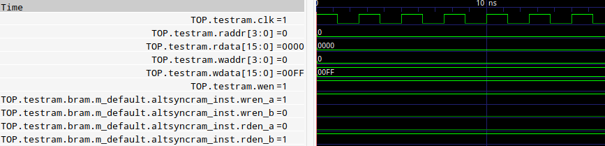
Now wren_a and rden_a both have the correct values. However, rdata is still not correct. What the ****!
To figure out the real root cause of this bug, I ran the simulation on VCS. VCS can generate the correct waveform when using the original simlib (i.e., the altsyncram directly from simlib, which contains a bunch of tri0 and tri1). However, with the version where all tri0 and tri1 are replaced with logic, VCS shows exactly the same result as verilator.
The problem is about tri0 and tri1. These are special wires that having a value z is also meaningful. When a wire with type tri0 has a value z, it is treated as 0; when a wire with type tri1 has a value z, it is treated as 1. Simply changing all tri0 and tri1 to logic may break the assumption that is held by a huge amount of codes in the implementation of altsyncram. In our case, in the module testram, a number of the interface wires of bram are left as unconnected; in verilator, the default value of these wires are 0.
The solution is to change testram to the following:
module testram(
    input logic clk,
    input logic wen,
    input logic [3:0] waddr,
    input logic [15:0] wdata,
    input logic [3:0] raddr,
    output logic [15:0] rdata
);

    altsyncram #(
        .intended_device_family("Stratix"),
        .operation_mode("DUAL_PORT"),
        .width_a(16),
        .widthad_a(4),
        .numwords_a(16),
        .width_b(16),
        .widthad_b(4),
        .numwords_b(16),
        .rdcontrol_reg_b("CLOCK0"),
        .address_reg_b("CLOCK0"),
        .outdata_reg_b("UNREGISTERED"),
        .read_during_write_mode_mixed_ports("OLD_DATA")
    ) bram (
        .clock0(clk),

        .wren_a(wen),
        .address_a(waddr),
        .data_a(wdata),
        .rden_a(0),

        .address_b(raddr),
        .q_b(rdata),
        .wren_b(0),
        .rden_b(1),

        .data_b(),
        .clock1(),
        .clocken0(1), // clocken0 was tri1
        .clocken1(1), // clocken1 was tri1
        .clocken2(1), // clocken2 was tri1
        .clocken3(1), // clocken3 was tri1
        .aclr0(0), // aclr0 was tri0
        .aclr1(0), // aclr1 was tri0
        .byteena_a(1), // byteena_a was tri1
        .byteena_b(1), // byteena_b was tri1
        .addressstall_a(0), // addressstall_a was tri0
        .addressstall_b(0), // addressstall_b was tri0
        .q_a(),
        .eccstatus()
    );
endmodule
In the above code, we manually assign a value to these “useless” wires. For the wires with a type tri0, we assign a value 0; for the wires with a type tri1, we assign a value 1. The simulation result is shown below.
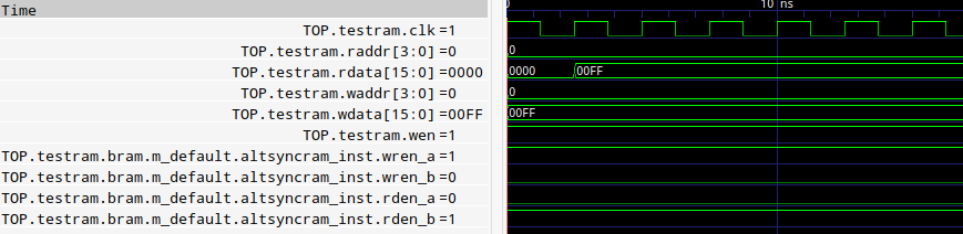
Everything is correct, and we can get the value!